• Opto-Electronic Science
  • Vol. 3, Issue 11, 230049-1 (2024)
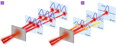
Shreeya Rane, Shriganesh Prabhu, and Dibakar Roy Chowdhury*
DOI: 10.29026/oes.2024.230049 Cite this Article
Shreeya Rane, Shriganesh Prabhu, Dibakar Roy Chowdhury. Physics and applications of terahertz metagratings[J]. Opto-Electronic Science, 2024, 3(11): 230049-1 Copy Citation Text show less
(a) The phenomenon of diffraction through conventional diffraction grating, where higher diffraction orders are present. (b) The diffraction phenomenon from metagrating where higher orders become evanescent in nature and only the zeroth order mode propagates light in the far-field.
Fig. 1. (a) The phenomenon of diffraction through conventional diffraction grating, where higher diffraction orders are present. (b) The diffraction phenomenon from metagrating where higher orders become evanescent in nature and only the zeroth order mode propagates light in the far-field.
(a) The schematic illustration of grating and the equivalent effective medium structure. When the grating is considered as homogeneous slab having effective refractive index, the grating region acts as a Fabry-Perot resonant cavity exhibiting multiple total internal reflections. The obtained transmittance characteristics of the proposed grating design for (b) TE and (c) TM polarization as a function of frequency. Here, the black solid line represents the transmittance acquired through numerical simulations while the red dotted line represents the transmittance obtained from experiment. The slight variation in the transmittance for both the polarizations (TE and TM) can be attributed to the different effective refractive indices for both the configurations. Figures reproduced from: ref.115, Elsevier B.V.
Fig. 2. (a) The schematic illustration of grating and the equivalent effective medium structure. When the grating is considered as homogeneous slab having effective refractive index, the grating region acts as a Fabry-Perot resonant cavity exhibiting multiple total internal reflections. The obtained transmittance characteristics of the proposed grating design for (b) TE and (c) TM polarization as a function of frequency. Here, the black solid line represents the transmittance acquired through numerical simulations while the red dotted line represents the transmittance obtained from experiment. The slight variation in the transmittance for both the polarizations (TE and TM) can be attributed to the different effective refractive indices for both the configurations. Figures reproduced from: ref.115, Elsevier B.V.
(a) The THz-TDS transmission signals have been observed under normal incidence. The solid curve represents bare Si, while the dashed and dotted curves depict Si coated with antireflection grating in TE and TM polarizations, respectively. (b) The amplitude and (c) phase shift of the complex reflective coefficient are measured at the Si/grating/air interface at 0.75 THz, with incidence being normal from the Si side. The noise level of the THz-TDS system is currently overlaid. Analytically calculated results for TE and TM waves at Cr thickness d = 30 nm are depicted as solid and dashed curves, respectively. Error bars are utilized to denote the geometric uncertainty arising from grating fabrication. Figures reproduced from: ref.123, Wiley-VCH GmbH.
Fig. 3. (a) The THz-TDS transmission signals have been observed under normal incidence. The solid curve represents bare Si, while the dashed and dotted curves depict Si coated with antireflection grating in TE and TM polarizations, respectively. (b) The amplitude and (c) phase shift of the complex reflective coefficient are measured at the Si/grating/air interface at 0.75 THz, with incidence being normal from the Si side. The noise level of the THz-TDS system is currently overlaid. Analytically calculated results for TE and TM waves at Cr thickness d = 30 nm are depicted as solid and dashed curves, respectively. Error bars are utilized to denote the geometric uncertainty arising from grating fabrication. Figures reproduced from: ref.123, Wiley-VCH GmbH.
(a) Schematic representation of a two-mode SMM used to depict the metagrating as a Mach-Zehnder interferometer without taking reflection of grating into account. Two-dimensional maps of the experimentally measured efficiencies of the grating device with frequency and angle for (b) TE and (c) TM configuration. In both the cases the metagrating is illuminated at Littrow angle of 46°. Figures reproduced with permission from: ref.124, under the terms of the Creative Commons Attribution License (CC BY).
Fig. 4. (a) Schematic representation of a two-mode SMM used to depict the metagrating as a Mach-Zehnder interferometer without taking reflection of grating into account. Two-dimensional maps of the experimentally measured efficiencies of the grating device with frequency and angle for (b) TE and (c) TM configuration. In both the cases the metagrating is illuminated at Littrow angle of 46°. Figures reproduced with permission from: ref.124, under the terms of the Creative Commons Attribution License (CC BY).
(a) Cross-sectional view of the proposed metagrating design and illustration of dynamic angle adaptive retroreflection. Modifying the period of the metagrating facilitates the provision of the desired momentum for various retroreflection angles. (b) The retroreflection efficiency obtained via simulated and experiment over a wide range of incident angles. (c) The reflective intensity distributions are assessed by measuring them from both an aluminium plate (used as a reference) and a retroreflector, considering various incident angles and periods respectively. Figures reproduced from: ref. 87, Wiley-VCH GmbH.
Fig. 5. (a) Cross-sectional view of the proposed metagrating design and illustration of dynamic angle adaptive retroreflection. Modifying the period of the metagrating facilitates the provision of the desired momentum for various retroreflection angles. (b) The retroreflection efficiency obtained via simulated and experiment over a wide range of incident angles. (c) The reflective intensity distributions are assessed by measuring them from both an aluminium plate (used as a reference) and a retroreflector, considering various incident angles and periods respectively. Figures reproduced from: ref. 87, Wiley-VCH GmbH.
(a) The top left figure denotes the complex refractive index of α-lactose sample, where the red and blue line represents real and imaginary part of the refractive index. The rest three figures denote the three surface coating instances for trace sample of equal volume. (b) The envelope corresponding to the angle-multiplexed reflectance spectra for conformal analyte coating and (c) The envelope associated with the angle-dependent reflectance spectra for evenly coated surface. The insets of the figure represents the normalized electric field distribution. Figures reproduced with permission from: ref. 129, under a Creative Commons Attribution 4.0 International License.
Fig. 6. (a) The top left figure denotes the complex refractive index of α-lactose sample, where the red and blue line represents real and imaginary part of the refractive index. The rest three figures denote the three surface coating instances for trace sample of equal volume. (b) The envelope corresponding to the angle-multiplexed reflectance spectra for conformal analyte coating and (c) The envelope associated with the angle-dependent reflectance spectra for evenly coated surface. The insets of the figure represents the normalized electric field distribution. Figures reproduced with permission from: ref. 129, under a Creative Commons Attribution 4.0 International License.
(a) Proposed metagrating design with a gold mirror at the back. The schematic denotes various parameters: θ signifies the incident angle, n denotes the number of angles, w represents the unit cell period, p indicates the grating layer width, h1 pertains to the height of the grating layer width, and h2 denotes the height of the waveguide layer. (b) Absorbance envelop of Ta2O5 thin film (1-µm thickness). (c) The fingerprint signal of the Ta2O5 film. Figures reproduced from: ref.132, IEEE.
Fig. 7. (a) Proposed metagrating design with a gold mirror at the back. The schematic denotes various parameters: θ signifies the incident angle, n denotes the number of angles, w represents the unit cell period, p indicates the grating layer width, h1 pertains to the height of the grating layer width, and h2 denotes the height of the waveguide layer. (b) Absorbance envelop of Ta2O5 thin film (1-µm thickness). (c) The fingerprint signal of the Ta2O5 film. Figures reproduced from: ref.132, IEEE.
The diffraction patterns of the experimentally acquired findings across the frequency spectrum from 0.2 THz to 0.9 THz after utilizing Fast Fourier Transform (FFT). The diffraction profile for TE incidence is shown by (a–c) for difference distances (10 μm, 20 μm, and 50 μm) away from the grating surface (along Z), whereas the diffraction profile for TM incidence is represented by (d–f). (g) and (h) illustrate the exponential decay characteristics of the +1 evanescent order, derived from experimental measurements for TE and TM cases, respectively. Here, the error bars signify variations in the experimental data, potentially arising from deformities during fabrication processes. Figures reproduced with permission from: ref.133, under the terms of the Optica Open Access Publishing Agreement.
Fig. 8. The diffraction patterns of the experimentally acquired findings across the frequency spectrum from 0.2 THz to 0.9 THz after utilizing Fast Fourier Transform (FFT). The diffraction profile for TE incidence is shown by (ac) for difference distances (10 μm, 20 μm, and 50 μm) away from the grating surface (along Z), whereas the diffraction profile for TM incidence is represented by (df). (g) and (h) illustrate the exponential decay characteristics of the +1 evanescent order, derived from experimental measurements for TE and TM cases, respectively. Here, the error bars signify variations in the experimental data, potentially arising from deformities during fabrication processes. Figures reproduced with permission from: ref.133, under the terms of the Optica Open Access Publishing Agreement.
(a) Illustrative depiction of graphene based reconfigurable metagrating. Results for two different cases where (b) μca=1.3eV and μcb=0.63eV, (c) μca=μcb=0eV with design parameters p = 60.926 µm, w = 19.4 µm, s = 5 µm, g = 2.9 µm, h = 8.5 µm, q = 0.05 µm. Here the blue, green and red lines represents the transmittance for 00, 0(–1) or 01 diffraction modes respectively. Figures reproduced from: ref.134, American Chemical Society.
Fig. 9. (a) Illustrative depiction of graphene based reconfigurable metagrating. Results for two different cases where (b) μca=1.3eV and μcb=0.63eV, (c) μca=μcb=0eV with design parameters p = 60.926 µm, w = 19.4 µm, s = 5 µm, g = 2.9 µm, h = 8.5 µm, q = 0.05 µm. Here the blue, green and red lines represents the transmittance for 00, 0(–1) or 01 diffraction modes respectively. Figures reproduced from: ref.134, American Chemical Society.
(a) Illustration of the polarization beam splitter constructed using a metallic metagrating. (b) Magnetic field configuration observed at an incident angle of θi = −30° for light polarized in the TM configuration. (c) The electric field configuration at an incident angle of θi = −30° for TE-polarized light. Figures reproduced with permission from: ref.136, under the terms of the Optica Open Access Publishing Agreement.
Fig. 10. (a) Illustration of the polarization beam splitter constructed using a metallic metagrating. (b) Magnetic field configuration observed at an incident angle of θi = −30° for light polarized in the TM configuration. (c) The electric field configuration at an incident angle of θi = −30° for TE-polarized light. Figures reproduced with permission from: ref.136, under the terms of the Optica Open Access Publishing Agreement.
(a) The schematic illustration of the metagrating design. (b) Simulated reflection spectra for metagrating submerged in solutions possessing various refractive indices. (c) The plot of wavelength value at absorption dip as a function of refractive index. Figures reproduced from: ref.137, OSA.
Fig. 11. (a) The schematic illustration of the metagrating design. (b) Simulated reflection spectra for metagrating submerged in solutions possessing various refractive indices. (c) The plot of wavelength value at absorption dip as a function of refractive index. Figures reproduced from: ref.137, OSA.
(a) Schematic representation of angle multiplexed metagrating. (b) A sequence of reflectance spectra obtained through angular scanning ranging from 16° to 25°, alongside their associated envelope curve, are presented for the metagrating coated with hBN. (c) The absorbance envelope curve and the reference absorbance spectrum of hBN. Figures reproduced with permission from: ref.131, De Gruyter, under the Creative Commons Attribution 4.0 International License.
Fig. 12. (a) Schematic representation of angle multiplexed metagrating. (b) A sequence of reflectance spectra obtained through angular scanning ranging from 16° to 25°, alongside their associated envelope curve, are presented for the metagrating coated with hBN. (c) The absorbance envelope curve and the reference absorbance spectrum of hBN. Figures reproduced with permission from: ref.131, De Gruyter, under the Creative Commons Attribution 4.0 International License.
Shreeya Rane, Shriganesh Prabhu, Dibakar Roy Chowdhury. Physics and applications of terahertz metagratings[J]. Opto-Electronic Science, 2024, 3(11): 230049-1
Download Citation